Encryption Block
John
Purba (john@students.ee.itb.ac.id)
The encryption block comprises 6 blocks:
-
Data & Key Input Register, interface of input data and
key
-
Key Expander, generator the round key
-
Control, controls each block
-
Rijndael Alg, implements Rijndael algorithm (round
calculations)
-
Data Output Register, interface of output data
The RTL VHDL code can be downloaded here enkrip.zip
The
encryption algorithm has been designed this way that the generation of round
key and the round calculations can be parallely executed. The advantage of this design is the
fact that we do not need to store the round key since they are currently
calculated. Interconnection of each block is depicted in figure 1.


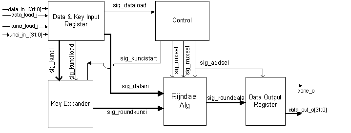
Figure 1
1. Data
& Key Input Register
This block is
data or key input interface. The length of data or key supported is 128 bits,
so we can use the same design for data input and key input. This block will
take 32 bits data and shifts them to next register. Four clock cycle will be
needed to take a complete 128 bit data. A simple controller is used here to
identify that a complete of 128 bits data has been accepted. The State Diagram
of FSMInput and Data or Key Input Register is depicted in figure 2.
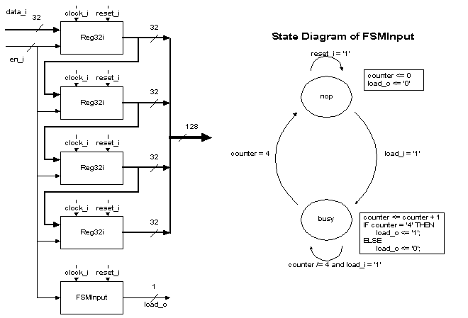
Figure 2
This block
takes 128 bit block data to output. First one block of 128 bits is divided to 4
blocks of 32 bits. One block of 32 bits data is take to output every one clock cycle.
Data output register is depicted in figure 3.
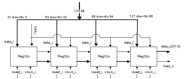
Figure 3
The Control block controls the Key Expander and Rijndael Alg block. The state diagram of Control block is depicted in figure 4.
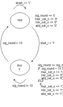
Figure 4
Key Expander responsible to generate round key for every round from the initial key. Based on the algorithm specification, if we use 128-bit key, 10 rounds will be needed. Hence the Key Expander will generate 10 round keys. The Key Expander is depicted in figure 5.
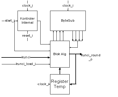
Figure 5
The Blok Alg implements the XOR operations and RotByte function.
Kontroler Internal controls the Key Expander and its state diagram illustrated
in figure 6. The ByteSub block is the same as ByteSub for Rijndael Alg Block.
State Diagram of Kontroler Internal
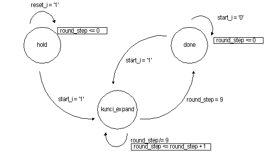
Figure 6
The
implementation of Rijndael Alg has been designed this way that it can work as
the initial round, standard round, and final round. The Rijndael Alg module is
depicted in figure 7.
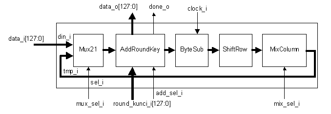
Figure 7
-
Mux21
Mux21 is a simple multiplexer 2 to
1. The format of data (din_i) is changed in this block, a block 128 bits sequence
to matrix 4x4 called State, as it is easier to design another blocks
(AddRoundKey, ByteSub, ShiftRow. MixColumn)
-
AddRoundKey
Implements AddRoundKey transformation,
a simple XOR between State and round key.
-
ByteSub
Implements ByteSub transformation,
contains 16 S-Box working in parallel. Dual Port Block RAM will be used to implements
2 S-Box, which emulate the ROM memory with configuration of 256x8 bits.
-
ShiftRow
Implements ShiftRow transformation.
The position of bytes in State will shifted cyclical by offsets. The first row
is shifted by zero, the second row is shifter by one, the third row is shifted
by two, and the fourth row is shifted by three. The implementation is realized
by hardwiring and do not need gate resource.
-
MixColumn
Implements MixColumn transformation.
The columns of State are viewed as the coefficients of polynomial over GF (28)
of degree smaller than three. This polynomial is multiplied by four terms fixed
polynomial a(x), {03)x3 + {01}x2 + {01}x + {02}, modulo
the polynomial x4 + 1.The multiplication with four terms fixed
polynomial can be simplified by using the matrix form. The implementation of
this transformation can be realized as shift and XOR operations.
Implementation Result
The
encryption algorithm has been implemented to FPGA Xilinx Virtex V300PQ240. It
has 20 Dual Port Block RAM to implement to ByteSub transformation. The
implementation parameters are:
-
Speed
The maximum frequency is 51 MHz
corresponds to throughput 298,899 Mbps.
-
Area
The design required 666 slices